Tutorial 1 [AM, Nov 8, 2010 (Monday)]
 |
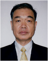
“An ultra low-power analog circuit and ADC design” Prof. Akira Matsuzawa |
Biography:
Akira Matsuzawa received B.S., M.S., and Ph. D. degrees in electronics engineering from Tohoku University, Sendai, Japan, in 1976, 1978, and 1997 respectively. In 1978, he joined Matsushita Electric Industrial Co., Ltd. Since then, he has been working on research and development of analog and Mixed Signal LSI technologies; ultra-high speed ADCs, intelligent CMOS sensors, RF CMOS circuits, and digital read-channel technologies for DVD systems. He was also responsible for the development of low power LSI technology and SOI devices. From 1997 to 2003, he was a general manager in advanced LSI technology development center. On April 2003, he joined Tokyo Institute of Technology and he is professor on physical electronics. Currently he is researching in mixed signal technologies; RF CMOS circuit design for SDR and high speed and ultra-low power data converters. He served guest editor in chief for special issue on analog LSI technology of IEICE transactions on electronics in 1992, 1997, and 2003, committee member for analog technology in ISSCC, vice program chair in SSDM, IEEE SSCS elected Adcom, IEEE SSCS Distinguished lecturer, educational program chair in A-SSCC, and vice president of Japan Institution of Electronics Packaging.
Abstract:
This talk will review and discuss an ultra low-power analog circuit and ADC design for portable medical electronics and green electronics. Ultra-low power analog circuits and mixed signal circuits, such as ADCs are required for long battery life or to address weak power supply. The conversion energy of ADC has been dramatically decreased by using non-OpAmp based dynamic analog circuit technique, such as SAR ADC. I will discuss the essence of non-OpAmp based dynamic analog circuit technique and compare it with the conventional OpAmp based analog circuit design. An analog operation with capacitances, digital mismatch and linearity compensation techniques, noise of dynamic comparator and its effect to the conversion accuracy will be covered. Also I will show an ultra low power (a few nW) capacitance to digital converter for capacitive pressure sensor, as an example of this technique. This technique must be very energy efficient method however looks difficult to increase the SNR. Then I will also discuss low noise amplification techniques and low power and high dynamic range delta-sigma modulation method which are still important for portable medical electronics.
Tutorial 2 [AM, Nov 8, 2010 (Monday)]
 |
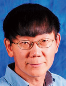
“Embedded Memory Design in Nano-Scale CMOS Technology” Dr. Kevin Zhang,
Intel |
Biography:
Kevin Zhang is an Intel Fellow and Director of Advanced Design at Logic Technology Development, Intel, where he is responsible to develop all critical technology and design collaterals, including design rules, digital library, analog and mixed-signal circuits, IO, and embedded memory for future product applications. Prior to this role, Zhang led the embedded memory technology development from 90nm to 32nm node at Intel. Zhang has published over 45 papers at international conferences and technical journals. He holds over 45 US patents in the area of integrated circuit technology. Currently, Zhang serves as Chair of ISSCC Memory Subcommittee. He received the BS and PhD degree in EE from Tsinghua University, Beijing and Duke University, respectively.
Abstract:
Embedded memory plays essential role in all modern VLSI systems. SRAM has been a main workhorse in meeting power and performance requirements. As CMOS technology scaling drives the feature size of transistor well into nano-scale regime, SRAM design is facing many key challenges in achieving both power and performance benefits while maintaining conventional density scaling trend. In this talk, the key challenges facing today's SRAM design will be thoroughly examined, including process variation, cell stability, and power management. The latest and most innovative design and technology solutions will be discussed in addressing these challenges. Some real product design examples based on the-state-of-the-art CMOS technologies will be analyzed to illustrate key design tradeoffs designers are facing today.
Tutorial 3 [PM, Nov 8, 2010 (Monday)]
 |
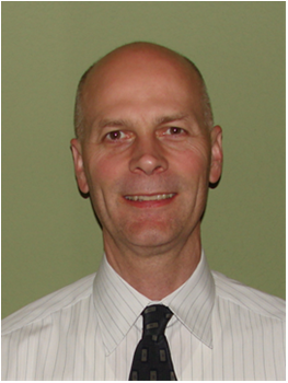
“Circuit-Level Power Management ” Dr. Gordon Gammie, Texas Instrument
|
Biography:
Gordon Gammie received bachelor degrees in physics and mathematics from Miami University, Oxford, Ohio, USA in 1985 and M.S. and Ph.D. in Electrical Engineering from the University of Illinois, Champaign, IL, USA in 1987 and 1991. In 1995 he joined Texas Instruments and has worked as a design and test engineer for multimedia ICs including video codecs, 3D graphics, and HDMI receivers and transmitters. Since 2002 Gordon has been part of the Chip Technology Center in the Wireless Division responsible for architecture and implementation of digital power management on mobile handset SoCs for 90, 65, 45, and 28nm CMOS. Gordon is a Distinguished Member of Technical Staff , holds 6 US patents and has 19 technical publications.
Abstract:
In the last couple of decades, handheld wireless devices (e.g. smartphones, e-readers, internet tablets, etc.) have become some of the most prolific electronic devices in history. With this has come an exploding demand for performance and features that cover almost every aspect of our digital multimedia interconnected lives. As ever increasing functions continue to be integrated into these products, there is an ongoing need to develop innovative ways to reduce power consumption and extend battery life. This talk will discuss these technology trends and challenges, as well as the circuit techniques designers are using today to reduce power. I will discuss static techniques for leakage reduction and adaptive techniques for active power reduction. State-of-the-art adaptive power management techniques such as adaptive voltage scaling, body bias, power gating, dynamic voltage-frequency scaling, and sleep modes, are discussed both in theory and through examples of implementations found in practice. Finally I’ll touch briefly on some of the challenges we face going forward.
Tutorial 4 [PM, Nov 8, 2010 (Monday)]
 |
“RF Integrated Circuit Design in Deep Submicron CMOS” Prof. John Long, TU Delft |
Biography:
John Long received the B.Sc. degree in electrical engineering from the University of Calgary, Canada, in 1984, and the M.Eng. and Ph.D.degrees in electronics from Carleton University,Ottawa, Canada, in 1992 and 1996, respectively. He was employed for 10 years by Bell-Northern Research, Ottawa (now Nortel Networks R&D) involved in the design of ASICs for Gbit/s fibre-optic transmission systems, and from 1996 to 2001 as an Assistant and then Associate Professor at the University of Toronto in Canada. Since January 2002 he has been Chair of the Electronics Research Laboratory at the Delft University of Technology in The Netherlands. His current research interests include transceiver circuits for integrated wireless and high-speed wireline data communications systems. Prof. Long is a former Associate Editor of the IEEE JOURNAL OF SOLID-STATE CIRCUITS, and is currently a Distinguished Lecturer for the IEEE Solid-State Circuits Society. He received the NSERC Doctoral Prize and Douglas R. Colton and Governor General’s Medals for research excellence, and is a co-recipient of Best Paper Awards from the International Solid-State Circuits Conference (ISSCC) in 2000 and 2007, the RFIC and EuropeanWireless Symposia in 2006, and IEEE-BCTM in 2003. He was general chair and local organizer for the 2006 IEEE Bipolar/BiCMOS Circuits and Technology Meeting (BCTM), held in Maastricht, NL. He chairs the RF circuits subcommittee for ISSCC 2010, andis a member of the technical program committees for the European Solid-State Circuits (ESSCIRC) and EuMIC conferences.
Abstract:
This tutorial addresses the design of basic radio front-end building blocks in advanced RF-CMOS for mobile, ultra-low power and broadband applications. Passive component design for RF circuits, including the modelling, design and implementation of inductors and transformers on-chip are described. ESD protection and packaging of RF circuits, including flip-chip and the electrical characteristics of plastic packages at RF are also detailed. Typical RF-CMOS building blocks such as low-noise amplifiers, mixers, frequency dividers, oscillators, and power amplifiers are used as design examples