|

 Tutorial 1
Silicon Microelectronic Chips in the Human Healthcare and Life
Scienc
Silicon CMOS
chips that make possible today’s computers are emerging as potential
new tools for rapid & sensitive electrical analysis of small
biological objects (cancer markers, bacteria, virus particles, and
DNA) in direct interface with them. A key potential advantage of the
interface between CMOS chips and bio systems is low production cost,
small size, and rapid analysis. The small, cheap, and fast CMOS
bioanalytical devices can contribute to lowering healthcare cost and
to facilitating fundamental biology study. In this tutorial, I will
review some exciting developments in the burgeoning area of making
CMOS-bio interfaces. A large amount of research is being done, and
the select review topics cannot be exhaustive, but they would
comprise an effective exposure to the field.
 |
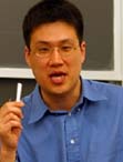
Donhee Ham
(Harvard Unviersity) |
Donhee Ham is Gordon McKay Professor of EE and Applied Physics at
Harvard. His research is on: (1) low-dimensional quantum plasmonics;
(2) applications of CMOS ICs in biotechnology; (3) soliton
electronics; (4) NMR quantum computing; (5) RF/analog/mixed-signal
ICs. He received the B.S. degree in physics from Seoul National
University in 1996, where he graduated summa cum laude with
Valedictorian Prize, Presidential Prize, and Physics Gold Medal,
ranked top 1st across Natural Science College. After a military
service in Korea, he proceeded to Caltech, where he first worked on
relativistic astrophysics under Barry Barish, and later obtained the
Ph.D. degree in EE in 2002, winning Wilts Prize, the best thesis
award in EE. His doctoral work examined the statistical physics of
circuits. He was the recipient of IBM Doctoral Fellowship, IBM
Faculty Award, IBM Design Award, KFAS Fellowship, Harvard Hoopes
prize, and MIT Technology Review Top 35 Innovator (TR35)
recognition. His experiences include LIGO, IBM Watson Center, IEEE
ISSCC & ASSCC TPCs, IEEE ISCAS advisory board, Nano/Biosystems
Institute advisory board, and industry/government advisory positions
on ultrafast electronics, nanoscale science, and interface between
biotechnology and circuits. He was a guest editor for IEEE JSSC and
a co-editor of CMOS Biotechnology with Springer.
 Tutorial 2
Inductive-Coupling Through-Chip Interface for 3D System Integration
When radio
communication range is shorter than 1/10 of the wave length, the
electromagnetic field exhibits unique characteristics. It is called
a near field. By using the near field radio vertical interface
through chips can be arranged in as high density as TSV (Through
Silicon Via). A wireless TSV that uses inductive coupling is
attracting attention. Although it is wireless, it bares comparison
with TSV in performance. Data rate per coil is over 10Gb/s. Energy
dissipation is below 1pJ/b, which is 1/10 of that in the
conventional high-speed serial links. Bit error rate is smaller than
10e-14. Above all, it is much inexpensive, since it is a circuit
solution in standard CMOS. Research in industry has started for
application study. It can be used for homogeneous and heterogeneous
chip stacking for SiP. It enables staking of 64 NAND flash memory
chips to realize a package-size SSD (Solid-State Drive). It raises
data rate and lowers power dissipation of high-speed DRAM interface.
Applications expand by extending communication ranges by enlarging
coil size, such as for bus probing of a microcontroller through a
package and non-contact wafer testing. Power supply can also be
delivered. This lecture will cover technologies and applications of
the inductive-coupling through-chip interface.
 |
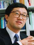
Tadahiro Kuroda
(Keio University) |
Tadahiro Kuroda received the Ph.D. degree in electrical engineering
from the University of Tokyo. In 1982, he joined Toshiba
Corporation. From 1988 to 1990, he was a Visiting Scholar with the
University of California, Berkeley. In 1990, he was back to Toshiba,
and invented and developed a Variable Threshold-voltage CMOS (VTCMOS)
technology and a Variable Supply-voltage scheme. In 2000, he moved
to Keio University, where he has been a professor since 2002. He was
a MacKay Professor at the University of California, Berkeley in
2006. His research interests include near field radio, image
recognition, and ultra-low-power CMOS design. He has published more
than 200 technical publications, including 60 invited papers, and 21
books/chapters, and has filed more than 100 patents. Dr. Kuroda
served as the General Chairman for the Symposium on VLSI Circuits,
the Vice Chairman for ASP-DAC, sub-committee chairs for A-SSCC,
ICCAD, and SSDM, and program committee members for the Symposium on
VLSI Circuits, CICC, DAC, ASP-DAC, ISLPED, and SSDM. He is a
recipient of the 2005 P&I Patent of the Year Award, the 2007 ASP-DAC
Best Design Award, and the 2009 IEICE Achievement Award. He is an
IEEE Fellow, IEEE SSCS Distinguished Lecturer, and an elected AdCom
member.
 Tutorial 3
Emerging ADC design
Most analog
IC designers and students are fascinated by and drawn to ADCs.
While some ADC realizations have had a lasting impact, examples
including pipelined ADCs with digital redundancy, flash ADCs with
folding and interpolation, and multi-bit delta-sigma modulators with
dynamic element matching, there are many more recent and emerging
ADC design techniques that are receiving much attention and also
gaining momentum in some areas. Many of these ideas are showered
with doubts and honest criticism. However, we may also be at a
juncture where a few of these developments may come to the rescue of
the tough submicron scaling challenge that we analog IC designers
face today. This tutorial will summarize and ponder the impact of a
few selective as well as random slices of these emerging ADC
designs.
 |
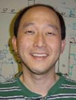
Un-Ku Moon
(Oregon State University) |
Prof.
Un-Ku Moon has been with the Oregon State University since 1998,
where he is currently a Professor. Prior to his arrival at OSU, he
was with Bell Labs 1988-1989 and 1994-1998. He received B.S. from
the University of Washington, M.Eng. from Cornell University, and
Ph.D. from the University of Illinois, Urbana-Champaign. He has
served as an Associate Editor of the IEEE JSSC and the IEEE TCAS-II,
as the Editor-in-Chief of the IEEE TCAS-II, and on the TPC of the
IEEE CICC. He also served on the IEEE SSCS AdCom and the IEEE CASS
BoG as the SSCS representative to CASS. He currently serves as the
Deputy Editor-in-Chief of the IEEE TCAS-II, and on the TPC of the
IEEE ISSCC and the IEEE VLSI Circuits Symposium.
 Tutorial 4
Advanced RF and Analog Design in the Nano-Meter Era
From a system
perspective, wireless transceivers are moving towards software
defined architectures. This means that wideband and flexible radio
frontends are needed which can receive and transmit many different
radio standards. Since there is a large amount of digital circuitry
involved, the technology in which these radios have to be designed
is nanometer scale CMOS. These technologies are optimized for high
density digital circuits and it's quite a challenge to design the
software defined architectures and the required circuits in these
technologies. In this presentation several analog and RF circuit
innovations will be given which take benefit from the properties of
nanometer scale CMOS. Topics: Thermal noise cancelling in
Balun-LNA-Mixer combination, ultra-linear filtering mixer, Polyphase
distortion compensation in a software radio transmitter, A wideband
harmonic rejection receiver architecture.
 |
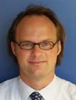
Bram Nauta (Twente
University) |
Bram
Nauta was born in Hengelo, The Netherlands. He received the M.Sc
degree and PhD Degree in electrical engineering from the University
of Twente, The Netherlands. From 1991 until 1998 he worked in
Philips Research labs where he worked on high-speed AD converters
and analog key modules. In 1998 he returned to the University of
Twente, as full professor heading the IC Design group. His current
research interest is analog and RF CMOS circuits.
Prof Nauta is member technical program committees of ISSCC, VLSI-
Symposium and ESSCIRC and currently the Editor in Chief of the IEEE
Journal of Solid-State Circuits.
---------------------------------------------------------------------------- - -
|


