
Panel Discussion
Tuesday, November 13
16:05-17:45
Panel Discussion 1: Disruptive design for emerging technology after 3D Devices/FinFET and beyond; How can we make it?
Panel Discussion 2: Challenge for Zero Stand-by Power Management- Road-map to the "Normally-Off Computing" -
Panel Discussion 1: Disruptive design for emerging technology after 3D Devices/FinFET and beyond; How can we make it?
| Organizer | Yung-Chow Peng, TSMC, Taiwan |
| Co-Organizer | Youngmin Shin, Samsung, Korea,South |
| Moderator | Toshiro Hiramoto, University of Tokyo, Japan |
| Panelist |
Aaron Thean, IMEC, EU Jae Cheol Son, Samsung, Korea, South Jong-Ho Lee, Seoul National University, Korea, South Philippe Magarshack, STM, France Sally Liu, TSMC, Taiwan Seiichiro Yamaguchi, Fujitsu, Japan Vinod Kariat, Cadence, USA |
Abstract:
Conventional technology before N28 follows scaling rule, device behaviors are not far away from projection.
Disruptive design could base on this projection to create disruptive design.
While technology enters into 3D/FinFET and beyond, device behaviors are complex and not similar as projection could be used before.
Besides process and design flow enhancement, is there any design solution could be used to break through this limitation?
A technology-matched disruptive design in time available becomes a challenge.
Is the digital assisted analog the most possible approach? Or dose the analog assisted digital with 3D IC benefit more?
In this panel, each specialist will talk about their research, technical and practical challenges from different domains.
And further we will be discussing approaches to break through the limitations on process, device behavior, design flow and co-optimization.
Organizer
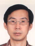
Yung-Chow Peng
TSMC, Taiwan
Co-Organizer
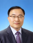
Youngmin Shin
Samsung, Korea,South
Moderator
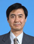
Toshiro Hiramoto
University of Tokyo, Japan
Position statement
The 22/20nm technology is at a turning point. No technology generation in the past has have so diversified device structures: planar bulk, planar FD SOI, and 3D FinFET. This diversity, unpredictable next generation technology, and more and more complex layout restrictions force difficult challenges on circuit design for 16/14nm and beyond. To break up conflicting requirements by more complicated device technology and more efficient circuit design, a paradigm shift in circuit design, or disruptive design, is mandatory.
This panel will be an excellent opportunity for device engineers and circuit designers to discuss disruptive design in 3D FinFET era and beyond. As a moderator, I will ask device engineers to disclose their visions on how emerging devices should be co-optimized with circuit design and circuit designers to raise their strong demands to device engineers on how disruptive design should happen under emerging technologies.
Biography
Toshiro Hiramoto received B.S., M.S., and Ph.D degrees in electronic engineering from the University of Tokyo in 1984, 1986, and 1989, respectively. In 1989, he joined Device Development Center, Hitachi Ltd. In 1994, he joined Institute of Industrial Science, University of Tokyo, Japan, as an Associate Professor and has been a Professor since 2002. His research interests include low power CMOS devices design, variability in scaled transistors, and silicon nanowire transistors.
Dr. Hiramoto is a fellow of Japan Society of Applied Physics and a member of IEEE and IEICE. He has served on Program Committee of Symposium on VLSI Technology since 2001 and will be the Program Chair in 2013. He was the Subcommittee Chair of CMOS Devices in 2005 and was an Executive Committee member in 2006-2009 in IEDM.
Panelist
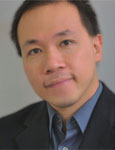
Aaron Thean
IMEC, EU
Position statement
As CMOS technology enters into an extremely difficult scaling regime post 20nm, challenged by patterning and performance, there is an even greater need to extract maximum value at the system/chip level, to leverage the high process cost. To meet the upcoming performance-power needs, disruptive post-FinFET technologies like Nanowire, will be needed to provide enhancement. Early design and process co-optimization can turn the disruptions to advantages. We will need a platform to exercise this new co-operative path-finding to define the coming technologies amidst the scaling challenges.
Biography
Aaron Thean is the Director of the Logic Device Program at IMEC, Aaron oversees the device R&D from ultra-scaled FinFETs to III-V/Ge Channels, and other novel emerging device architectures. Prior to joining IMEC in 2011, he was one of Qualcomm's 20nm technologists and managers. He had also served as IBM's 28nm/32nm Front-End-of-Line Device manager, and Freescale's Novel Device Manager. As an alumni of the University of Illinois at Champaign-Urbana, he received his B.Sc.(Highest Honors), M.Sc, and Ph.D degrees in Electrical Engineering. He has published over 45 peer-reviewed papers currently holds more than 42 U.S. patents on advanced semiconductor technology and processes.
Panelist
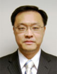
Jae Cheol Son
Samsung, Korea, South
Position statement
Scaling beyond 20nm requires fully-depleted (FD) device to overcome short channel effects. Superior sub-threshold slope and drain induced barrier lowering characteristics of FD device allow threshold voltage to be lowered at same leakage as planar device. Although there are several main FD device architectures, bulk FinFET seems to be the most cost-effective option for the near-term. Expectation is that FinFET technology will enable more energy-efficient SoCs than conventional planar technology.
Biography
Dr. Jae Cheol Son is VP of SoC Processor Development Team at Samsung Electronics, where he leads the high-performance CPU and GPU processor development. His R&D interests include high-performance microprocessor and VLSI design, graphics and multimedia processing, and statistical signal processing. He received master and doctoral degrees in electrical engineering from KAIST, Korea.
Panelist
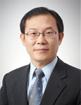
Jong-Ho Lee
Seoul National University, Korea, South
Position statement
The age of integrated circuit (IC) design using tri-gate MOSFETs (or FinFETs) is on its way. Compared to conventional planar channel devices, tri-gate transistors are known to give better performance with scaling-down. In 2011, Intel reported successful mass production of new CPU using tri-gate MOSFETs (or bulk FinFETs). In this panel, bulk and SOI FinFETs as 3-D MOSFETs will be compared briefly and their key properties are introduced in terms of integrated circuit design. It is important to consider key parameters like parasitic capacitance, parasitic S/D resistance, back-bias effect, and low frequency noise in the design of ICs using 3-D transistors. The limitation of heat dissipation has an effect on integration density of ICs. Therefore device temperature for both SOI and bulk FinFETs has to be considered. Physical layout of ICs using 3-D transistors may be different from that of conventional IC design. When 3-D transistors are used in IC design, the design needs to be compact as possible without triggering latch-up.
Biography
Jong-Ho Lee received the Ph.D. degree from Seoul National University, Seoul, in 1993, in electronic engineering. In 1994, he was with the School of Electrical Engineering, Wonkwang University, Iksan, Chonpuk, Korea. In 2002, he moved to Kyungpook National University, Daegu Korea, as a Professor of the School of Electrical Engineering and Computer Science. Since September 2009, he has been a Professor in the School of Electrical Engineering, Seoul National University, Seoul Korea. From August 1998 to July 1999, he was with Massachusetts Institute of Technology, Cambridge, as a postdoctoral fellow. He has authored or coauthored more than 160 papers published in refereed journals and over 280 conference papers related to his research and has been granted ~90 patents in this area. His research interests include CMOS technology, non-volatile memory devices, thin film transistors, sensors, bio interface, and neuromorphic technology. He has been served as a subcommittee member of IEDM, ITRS ERD member, a general chair of IPFA2011, and IEEE EDS Korea chapter chair. In 2006, he was a recipient of the "This Month's Scientist Award" for his contribution in the development of practical high-density/high-performance 3-dimensional nano-scale CMOS devices. He invented Saddle FinFET (or recess FinFET) for DRAM cell and NAND flash cell string with virtual source/drain, which have been applying for mass production.
Panelist
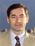
Philippe Magarshack
STM, France
Position statement
While there is consensus in the semiconductor world, that fully-depleted transistors have to replace conventional transistors at 20nm or below, most of the industry is embarking on 3D transistors (or FinFETs). ST is pioneering the usage of the alternative fully-depleted device, also known as Ultra-Thin-Body-Box Fully-Depleted SOI (UTBB FDSOI). This FDSOI transistor has the same electrical benefits as the FinFETs, (including electrostatic control of the channel) while retaining a conventional planar structure, with benefits in manufacturability and silicon costs, and also in designer friendliness. FDSOI's additional capabilities of Forward- and Reverse- Body Biasing make it a unique platform for high energy efficiency products for Wireless and Consumer applications. We believe that FDSOI will extend its benefits from 28nm to 14nm, and possibly 10nm.
Biography
Magarshack is Corporate Vice President of STMicroelectronics in charge of Design Enablement & Services and has held this position since February 2012. From 1985 to 1989, Magarshack worked as a microprocessor designer at AT&T Bell Labs in the USA. In 1989, he joined Thomson-CSF in Grenoble, France, and took responsibility for libraries and ASIC design kits for the military market. In 1994, Magarshack joined the Central R&D Group of SGS-THOMSON Microelectronics (now STMicroelectronics), where he has held several roles in CAD and Libraries management for advanced integrated-circuit manufacturing processes. In 2005, Magarshack was promoted to Group Vice President and General Manager of Central CAD and Design Solutions at STMicroelectronics' Technology R&D and Manufacturing organization. Magarshack is ST's Enablement Executive at the IBM ISDA Technology Alliance for the development of advanced CMOS process. He sits on the boards of Silicon Integration Initiative (Si2) and ENSIMAG Engineering School in Grenoble.
Panelist
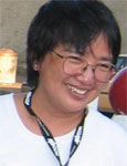
Sally Liu
TSMC, Taiwan
Position statement
The emerging technologies have multi-faucets. To deliver the full advantages of these emerging technologies, a paradigm shift to system centric design is a must. To cope with the uncertainty in emerging technologies, an open flexible EDA platform is required to rein in the newly observed nanometer effects and deliver energy efficiency.
Biography
Sally Liu is Technical Director of MS/RF Solutions Division at TSMC. Dr. Liu joined TSMC in 2004, after years at Bell Laboratories, Conexant and RF Integrated Corporation, specialized in modeling & simulation, characterization and design flows. Her professional interests include emerging nanometer devices, 3D IC, statistical modeling and design centering.
Panelist
Seiichiro Yamaguchi
Fujitsu, Japan
Position statement
Who desires disruptive design that will require designers to change well established design flow or methodology to use the coming technology? Even though 3D Devices/FinFET behaviors are not similar to the conventional technology, impact to the design methodology should be minimized.
Biography
He received his B.E. degree in Applied Physics from Waseda University in 1985.He joined Fujitsu limited in 1985 and had worked in the field of the modelingand simulation of devices. Since 1999, he has been engaged in the developmentof advanced CMOS technologies. Currently, he is the Deputy General Manager ofTechnology Development Division.
Panelist
Vinod Kariat
Cadence, USA
Position statement
Designing at advanced CMOS nodes today requires us to deal with multiple conflicting trends: a) transistors at advanced CMOS nodes (28nm and below) are increasingly unfriendly to analog design requirements, b) only few sockets are available for large scale SOCs and only few companies can afford to design at these advanced nodes, and c) for those who can afford to design at these nodes, transistors are cheap and plentiful, but schedules are tight. Economics will drive practical design tradeoffs that will enable us to leverage advanced nodes where it makes sense, but not across the board as in the past.
Biography
Vinod Kariat is currently Fellow and Vice President of R&D at Cadence Design Systems, where his responsibilities include custom layout automation and library characterization. Dr. Kariat has worked in various management and technical positions at Cadence since 2001, and has a broad background in design automation. Prior to joining Cadence, Dr. Kariat was co-founder and VP of R&D at CadMOS Design Technologies, where he pioneered on-chip static noise analysis. Dr. Kariat has a PhD in computer engineering, is a senior member of IEEE and holds 14 US patents.
Panel Discussion 2: Challenge for Zero Stand-by Power Management- Road-map to the "Normally-Off Computing" -
| Organizer | Kazutami Arimoto, Okayama Prefecture University, Japan |
| Co-Organizer | Toru Shimizu, Renesas Electronics, Japan |
| Moderator | Hiroshi Nakamura, University of Tokyo, Japan |
| Panelist |
Shinobu Fujita, Toshiba, Japan Hoi Jun Yoo, KAIST, Korea, South Masanori Hayashikoshi, Renesas, Japan Hiroaki Takada, Nagoya University, Japan Steven Bartling, TI, USA Bert Gyselinckx, IMEC, EU Shey-shi Lu, National Taiwan Unversity, Taiwan |
Abstract:
System level Green innovations, including Medical and Health-care Appliances, Smart City, Smart Car, and Smart Home etc. are expected to bring us more comfortable and higher-quality human life, but further energy efficiency is required for those systems to meet the expectation.
"Normally-Off Computing" is believed as one of the most promising ways to satisfy the requirement.
In Japan, Normally-Off Computing Project started at September 2011 under the supported of NEDO (New Energy and Industrial Technology Development Organization) and METI (Japanese Minister of Economy, Trade and Industry).
Currently, The University of Tokyo, Renesas, Toshiba, and Rohm are leading this project in collaboration with 8 universities and national research institute to the goal of "Normally-Off Computing".
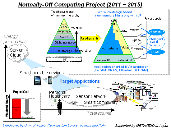
Under the ideal normally-off computing, all the components of computer systems are completely powered off whenever they need not to operate, and hence Stand-by Power is not consumed at all. There remain, however, a lot of problems to be solved with tight collaboration of wide range of design layers including device, circuits, architecture, software, and applications.
In this panel, world leading engineers and researchers in these fields are invited and present their own visions on the expectation and challenges to the "Normally-Off Computing".
Organizer
Kazutami Arimoto
Okayama Prefecture University, Japan
Co-Organizer
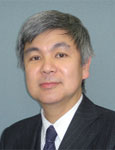
Toru Shimizu
Renesas Electronics, Japan
Moderator
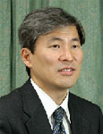
Hiroshi Nakamura
University of Tokyo, Japan
Position statement
Power consumption is one of the most sever design constraint in system LSI designs. Normally-off computing which completely shut down the power of all the components when not used seems one of the most promising ways to solve this problem. Effective performance of the current VLSIs does not improve as much as the production of the number of transistors and its clock frequency. This indicates that the room for normally-off is increasing in the current computing. However, in order to realize zero stand-by power management, we need further sophisticated power control mechanisms including how, when and where to power off. Innovations of circuits and/or device technology certainly provides better methods how to power off, but they cannot solve all the problems because the activity within a VLSI is determined not by circuits and/or device technology but by architecture, software, and applications. Thus, tight collaboration of wide range of design layers is indispensable to reach the goal of true normally-off computing.
Biography
Hiroshi Nakamura is a Professor at the Department of Information Physics and Computing in the Graduate School of Information Science and Technology at The University of Tokyo. He received the Ph.D. degree in Electrical Engineering from The University of Tokyo in 1990. His research interests include power-efficient computer architecture and VLSI design for high-performance and embedded systems. He led the project of "Innovative Innovative Power Control for Ultra Low-Power and High-Performance System LSIs" supported by JST (Japan Science and Technology Agency) from 2007 to 2012, and is now leading the "Normally-Off Computing Project" supported by NEDO/METI. He is a senior member of IEEE and ACM.
Panelist
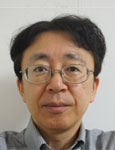
Shinobu Fujita
Toshiba, Japan
Position statement
Nonvolatile Memory Device
For the first time, we have demonstrated very fast switching speed and very small switching energy at the same time using an advanced STT-MRAM, meaning that SRAM-based cache memory can be replaced by our STT-MRAM. We already proposed a new memory hierarchy with volatile/nonvolatile hybrid using STT-MRAM for effective power reduction for real applications running on mobile processors. This idea can be realized by the advanced STT-MTAM, which is a big step toward normally-off computing for high-performance systems. Through this work, it was clarified that"Zero-standby Power" is not equivalent to "Low-Power", and"All Nonvolatile Memory Hierarchy" is not suitable for high performance processor.
Biography
Chief Research Scientist of Toshiba Corporate R&D Center.
He is leading a STT-MRAM based normally-off processors for mobile-SoC in a NEDO normally-off computing systems in Japan.
Panelist
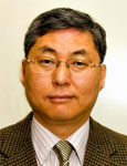 Hoi Jun Yoo
KAIST, Korea, South
Position statement
Mobile/Network SoC
Human brain consumes less than 20W while processing more complex computations such as recognition, mining, and synthesis of human experience compared with Intel Core i7, consuming 65W. This is possible due to low power-density (~15mW/cm3) and high neuron-density (70 million/cm3) of human brain enabling massive parallel computing even though each neuron processes slowly. Therefore brain-mimicking approaches based on neural networks should be exploited to implement ultra-low power consumption for high performance portable systems.
Biography
Hoi-Jun Yoo (M'95 - SM'04 - F'08) graduated from Electronic Department of Seoul National University and received MS and Ph.D. degrees from Electrical Engineering, KAIST. He was the VCSEL pioneer in Bell Communications Research at Red Bank, NJ. USA and Manager of DRAM design group at Hyundai Electronics designing from 1M DRAM to 256M SDRAM.Currently, he is a full professor of Department of Electrical Engineering at KAIST and the director of the System Design Innovation and Application Research Center (SDIA). From 2003 to 2005, he served as the full time Advisor to the Minister of Korean Ministry of Information and Communication for SoC and Next Generation Computing. His current research interests are Bio Inspired IC Design, Network on a Chip, Multimedia SoC design, Wearable Healthcare Systems, and high speed and low power memory. He has published more than 250 papers, and wrote or edited 5 books, "DRAM Design"(1997, Hongneung), "High Performance DRAM"(1999 Hongneung), "Low Power NoC for High Performance SoC Design"(2008, CRC), "Mobile 3D Graphics SoC"(2010, Wiley), and "BioMedical CMOS ICs"(Co-editing with Chris Van Hoof, 2010, Springer), and many chapters of books. Dr. Yoo received the Korean National Medal for his contribution to Korean DRAM Industry in 2011, the Electronic Industrial Association of Korea Award for his contribution to DRAM technology the 1994, Hynix Development Award in 1995, the Korea Semiconductor Industry Association Award in 2002, Best Research of KAIST Award in 2007, Design Award of 2001 ASP-DAC, Outstanding Design Awards of 2005, 2006, 2007, 2010, 2011 A-SSCC, and Korean Scientist of the Month Award (Dec. 2010). He is a member of the executive committee of Symposium on VLSI, and A-SSCC. He was the TPC chair of the A-SSCC 2008, a guest editor of IEEE JSSC and IEEE T-BioCAS. He was the TPC Chair of ISWC(International Symposium on Wearable Computer) 2010, IEEE Fellow, IEEE Distinguished Lecturer('10-'11), Far East Chair of ISSCC(�e10-�e11), and currently ISSCC Technology Direction Sub-committee Chair and an associate editor of IEEE TCAS-II.
Panelist
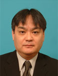
Masanori Hayashikoshi
Renesas Electronics, Japan
Position statement
Normally Off computing architecture
As the challenge for further low-power consumption, there is the fusion for technology of non-volatile memory (NV-RAM) and Normally-Off Computing. That is, in order to realize aggressively powered off whenever they need not to operate, localized the task processing on the time axis, and maximized the power-off time. The system architecture which has the co-design of hardware and software is one of key issues for Normally-Off Computing. Our challenge of Normally-Off computing architecture will be discussed, here.
Biography
Masanori Hayashikoshi was born in Ehime, Japan, on December 7, 1961. He received the B.S. and M.S. degrees in electronic engineering from Kobe University, Kobe, Japan, in 1984 and 1986, respectively.
In 1986, joined the LSI Research and Development Laboratory, Mitsubishi Electric Corporation, Hyogo, Japan. He is currently a Chief Engineer of Embedded Memory Core Development Div. in Renesas Electronics Corporation. Since 1986, he has been engaged in the research and development of EEPROM's, high density DRAM's, Low power SDRAM's, embedded MRAM's for MCUs, and Normally-Off computing architecture as the challenge for further low-power solution with NVRAM.
Panelist
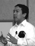
Hiroaki Takada
Nagoya University, Japan
Position statement
Normally Off computing Software
Though we beleive that "Normally-Off Computing" is one of the promising approach to reduce energy consumption of computing systems, there are little work necessary for system software researchers and engineers for the technology. We are looking forward to hear various requirements on system software for "Normally-Off Computing".
Biography
Hiroaki Takada is a Professor at the Department of Information Engineering, the Graduate School of Information Science, Nagoya University. He is also the Executive Director of the Center for Embedded Computing Systems (NCES). He received his Ph.D. degree in Information Science from University of Tokyo in 1996. His research interests include real-time operating systems, real-time scheduling theory, automotive embedded systems, and embedded system design. He is the leader of the TOPPERS Project, a project to develop open-source real-time operating systems for embedded systems.
Panelist
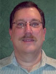
Steven Bartling
TI, USA
Position statement
Bio/Medical/Health Application Platform
Existing patient monitoring techniques can often be intrusive and interfere with the collecting of viable data, leading to inaccurate diagnosis. In sleep studies for example, sensors and wiring make patients uncomfortable and interfere with normal sleep patterns. Without a dramatic change in system design approaches, untethered ambulatory patient monitoring will not be possible. Exploiting the combination of embedded intelligence (MCU's + accelerators), embedded ULP NVM and the emerging normally-off computing paradigm will be necessary to meet these challenges.
Biography
Steven Bartling is the Technology Development Manager in the MCU Business Unit at Texas Instruments. His current research interests include ultra low power logic and memory circuits, processor architectures and system design. In the past, he has had key roles in the development of RISC 29000, PowerPC and x86 compatible CPU's.
Panelist

Bert Gyselinckx
IMEC, EU
Position statement
Sensor Network Application Platform
"Wearable device are enablers for a healthier lifestyle leading to improved quality of life. In order to live up to this promise, these devices have to operate energy autonomously throughout their lifetime - who would be willing to unplug 10's of devices out of her clothing, glasses, watches every night to charge overnight? Normally off computing with zero stand by power is a must. Especially in the domain of non volatile memories and power switching a lot of gain can be made. Next to this, we will also require new architectures that focus on energy autonomy - balancing available energy n the system with the quality of service of the wearable devices."
Biography
Bert Gyselinckx is currently General Manager of Holst Centre - imec. Bert was instrumental in defining the technical strategy of the Holst Centre at its creation in 2005. He brought to the Holst Centre his program management experience and know how in wireless research from IMEC.
Bert is well known in the scientific community for his pioneering contributions to wireless OFDM communications leading to our current generation of WiFi modems. Bert lives by the golden rule "working hard, playing hard". In 2001, he replaced his office chair for a bike saddle and went on a 12 month odyssey in the Asia Pacific region. After 15000km in "under" developed countries, he was inspired to create technologies that can have a true impact on society.
For this purpose, he established the Human++ program within imec. This program develops disruptive technologies for health and comfort monitoring. As the exponent of the Human++ program, Bert became known as a thought leader in the area of body area networks.
Bert received the M.S. degree in Electrical Engineering from the Rijksuniversiteit Gent, Belgium, in 1992 and the DEA degree in Air and Space Electronics from the École nationale supérieure de l'aéronautique et de l'espace, Toulouse, France, in 1993. At this time, he was also a trainee at the Research and Development group of Siemens in Munich, Germany.
Panelist
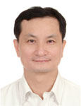
Shey-shi Lu
National Taiwan Unversity, Taiwan
Position statement
Medical Applications for Normally off Computing
System-on-a-chip has made great progress and found a lot of applications in past decades. However, in most cases, the quantity needed for a specific medical application does not justify the use of this advanced technology for the goals of low cost and power. With the advent of normally off computing, a common micro-chip, which we called human black box (HBB), for various medical applications, can be implemented in mass-production lines. Combined with machine-to-machine technology, the concept of internet of medical things for off-the-body, on-the-body, and inside-the-body applications using normally off computing will be discussed.
Biography
Shey-Shi Lu is a professor in the department of Electrical Engineering, National Taiwan University (NTU), associate director of Intel-NTU Connected Context Computing Center, and coordinator of medical electronics projects in National Program for Intelligent Electronics (NPIE), Taiwan. His recent research interests include CMOS Bio-MEMS/nanowire DNA/protein/glucose sensing SoC, CMOS drug delivery SoC, CMOS nerve stimulating SoC for pain control, and CMOS gas detection SoC for human breath analysis.