
Tutorial
Monday, November 12
Tutorial I 9:30-12:25
SoC Power Reduction and Management Techniques

Stefan Rusu
Intel, USA
Abstract
CMOS process technology scaling has enabled higher feature integration in system-on-chip with multiple CPU and graphics cores and larger on-die caches.
Reducing and managing power consumption is the most challenging task in today's highly complex systems.
In this tutorial, we will review power reduction and management techniques implemented in recent microprocessor and SoC designs, covering the entire spectrum from server to handheld applications.
We will review flip-flop power optimization techniques, clock loading reduction, low-voltage operation, leakage reduction techniques, dynamic voltage and frequency scaling, and fine-grain power management techniques.
Special attention will be devoted to adaptive circuit techniques that reduce the voltage and frequency design guard-bands.
This tutorial includes recent innovations and practical examples from both industry and academic research
Biography
Stefan Rusu received the MSEE degree from the Polytechnic University in Bucharest, Romania. His industry experience includes 20 years with Intel Corp. and 6 years at Sun Microsystems. He is presently a Senior Principal Engineer in Intel's Microprocessor and Graphics Division leading the technology and special circuits design for the Xeon® Processors. Stefan has authored over 90 papers on VLSI circuit technology and holds 35 U.S. patents. He is an IEEE Fellow and a member of the Technical Program Committee for ISSCC, ESSCIRC and A-SSCC conferences. Stefan is an Associate Editor of the IEEE Journal of Solid-State Circuits and an elected member of the SSCS AdCom.
Tutorial II 9:30-12:25
Designing CMOS Wireless LAN System-on-a-Chip

Srenik Mehta
Qualcomm Atheros, USA
Abstract
Wireless LAN SoCs are ubiquitous today in mobile, computing, and consumer electronics.
The simultaneous push for low-cost and high-performance has necessitated the use of scaled CMOS technology with extensive use of digital calibration.
This tutorial provides an overview of the challenges in designing CMOS wireless LAN System-on-a-Chip from the perspective of an analog/RF designer.
An overview of transceiver building blocks, integration issues, and calibration techniques are described.
Two system-on-a-chip examples are presented to contrast the techniques required for low-cost highly integrated 1x1 WLAN SoC versus a high-performance 3x3 WLAN SoC.
Biography
Srenik Mehta is a Sr Director of Engineering at Qualcomm Atheros, where he is engaged in the development of analog, mixed-signal and RF integrated circuits for wireless communication products. Srenik received the B.S. and M.S. degrees in electrical degrees in electrical engineering from the University of California, Berkeley, in 1992 and 1997, respectively. From 1995 to 2000, he worked as a Senior Design Engineer at Level One Communications (now Intel Corporation), San Francisco, CA, where he designed CMOS RF and mixed-signal ICs for cordless telephones. Since February 2000, he has been with Atheros Communications (now Qualcomm Atheros), San Jose, California. He has been serving on the RFIC Symposium technical committee since 2005.
Tutorial III 13:25-16:20
High Performance Non-Volatile Memory Design in Nano-Scale Era

Dr. Sungdae Choi
SK hynix
Abstract
Increase in the digital multimedia appliances such as mp3 player, digital camera brought huge demand for large capacity non-volatile memory (NVM) as a mobile storage device. And Solid-Sate Disk (SSD) is also getting into the spotlight. NAND Flash memory occupies the biggest portion among the non-volatile memory devices due to the small cell size and the maturity of the fabrication process, although it has the inherent disadvantage such as the slow write time and need of extra operations. Emerging NVM devices such as PCRAM and magnetic RAMs are expected as the next generation NVMs which succeeds the NAND Flash memory. This tutorial covers the problems and breakthrough of NAND Flash memory, introduction of expecting NVM devices and shows how they can work together to achieve the synergy effect.
Biography
Sungdae Choi received the B.S., M.S. and Ph.D. degrees from KAIST, Daejeon, Korea, in 2001, 2003 and 2006, respectively. His research field included application-specific-memory applications and body sensor network architecture. From 2006 to 2008, he joined Sakurai Lab. in the university of Tokyo, Japan, as a post-doctoral researcher and worked for the design for manufacturability project. From 2008 to 2009, he joined KAIST as a post-doctoral researcher and wrote the book titled Revised DRAM Design which will be published in 2012. In 2009, he joined SK hynix where he is currently working as a senior engineer at the Flash Development Division. Recently, he is also serving as a technical program committee member of ISSCC and ASSCC.
Tutorial IV 13:25-16:20
Smart Sensor Design in Standard CMOS
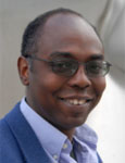
Prof. Kofi Makinwa
Delft Univisity of Technology
Abstract
Smart sensors are everywhere! They can be found in our homes, our cars and in nearly all mobile phones. However, processing weak sensor signals is quite challenging, especially when it must be done in standard CMOS, whose precision is limited by 1/f noise, component tolerances and mismatch. In this tutorial, a system approach to the design of smart sensors will be presented. The use of dynamic techniques, such as chopping, auto-zeroing, dynamic element matching and sigma-delta modulation, to trade speed for precision will be discussed. Examples will be given of state-of-the-art CMOS smart sensors for the measurement of temperature, humidity, magnetic field and even wind velocity.
Biography
Kofi A.A. Makinwa is a Professor at Delft University of Technology, where he leads a group that designs precision analog circuits, ΣΔ modulators, and smart sensors. This has resulted in 4 books, 17 patents and over 160 technical papers, many of which have received best paper awards: from the ISSCC, ESSCIRC, Transducers and JSSC among others. Dr. Makinwa has presented tutorials at several conferences and has served on the TPC of ISSCC and as an IEEE distinguished lecturer. He is currently on the TPC of ESSCIRC and the Advances in Analog Circuit Design (AACD) workshop, He is an IEEE fellow and an elected member of the IEEE SSCS AdCom.